The amount of sophisticated technology packed into a modern digital single lens reflex camera is simply astounding. In this article we’ll look at three of a DSLR camera’s most scientifically interesting components: the SLR mechanism itself, the camera lens motor, and the image sensor.
Single Lens Reflex
A single lens reflex (SLR) system allows the photographer to see the exact same image through the viewfinder as what is received by the image sensor and recorded. It does this using a hinged mirror (Fig. 1, solid green). While the photographer is composing and focusing, the image passes through the lens, reflects off the 45° mirror and passes through the pentaprism (yellow) to the eyepiece. When the shutter button is depressed, the mirror swivels up out of the way (dashed green) and the light travels directly to the image sensor (red).
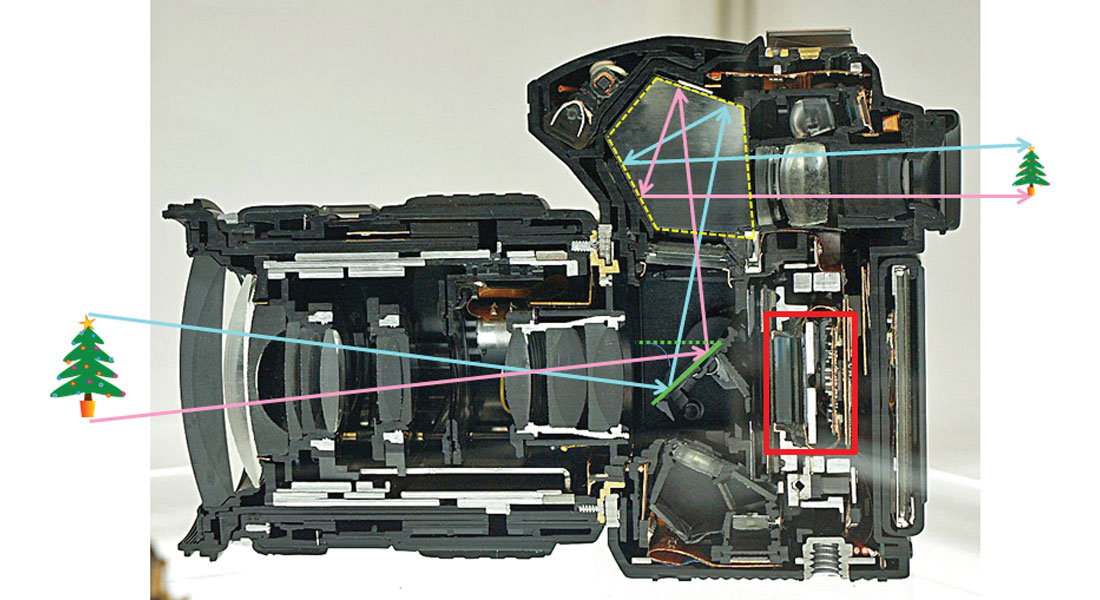
If the photographer prefers to use the LCD view screen instead of the eyepiece, the mirror is flipped up, and instead of recording the image, the image sensor sends the digital signals to the LCD screen.
If you look carefully at Figure 1 you will see a small mirror behind the main mirror. The main mirror is actually a beamsplitter, allowing some light to pass though it to reflect down to the autofocus (AF) mechanism at the bottom of the camera. The AF system is very complex, but briefly, this is how it works. The light passes down through masks which isolate two small zones of light from different sides of the lens. These two beams of light then pass through their own separate AF lenses and are projected onto linear arrays. As the main lens motor moves, the two array patterns change; when the two patterns inversely match, the main lens is in focus. All this is done in a couple of milliseconds! AF systems can also determine the velocity of the subject in order to anticipate the correct focus when the image is recorded, which of course is slightly in the future.
Lens Motors
How does the AF system move the lens so quickly and precisely in response to the information it receives as described above? There is a motor in every AF lens, and how it works is extremely interesting. Early AF lenses were mechanically driven by a motor housed in the camera body itself. In the late 1980’s ultrasonic motor (USM) technology was developed in Japan with Canon leading the way, and today USM’s are ubiquitous, found even in lower priced cameras.
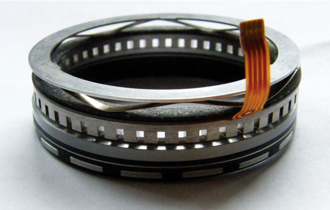
USM’s can be either linear or rotational, and cameras use the latter. A toothy stator ring has an outer layer of piezo-electric ceramic material bonded to it, typically lead zirconate titanate, and located next to it is a rotor ring. When a high frequency (~20-100 KHz) AC current is applied to the stator it creates a standing resonant wave. If two currents of different phase are applied, then the combination of the two standing waves creates a travelling wave on the surface of the stator with an amplitude of just a few nanometers (Figure 2). In the figure the travelling wave moves to the right, but the retrograde motion of the wave crests moves the rotor to the left, via static friction. Stators typically are toothed, as this creates a cilia-like effect as the tips of the teeth experience their elliptical retrograde movement, pushing the rotor to the left. Figure 3 shows a real camera USM with the AC voltage wires visible, as well as the spring that forces the stator and rotor together. The force of the spring is strong enough to prevent movement with no voltage, but not too strong to prevent the USM from doing its thing when powered.
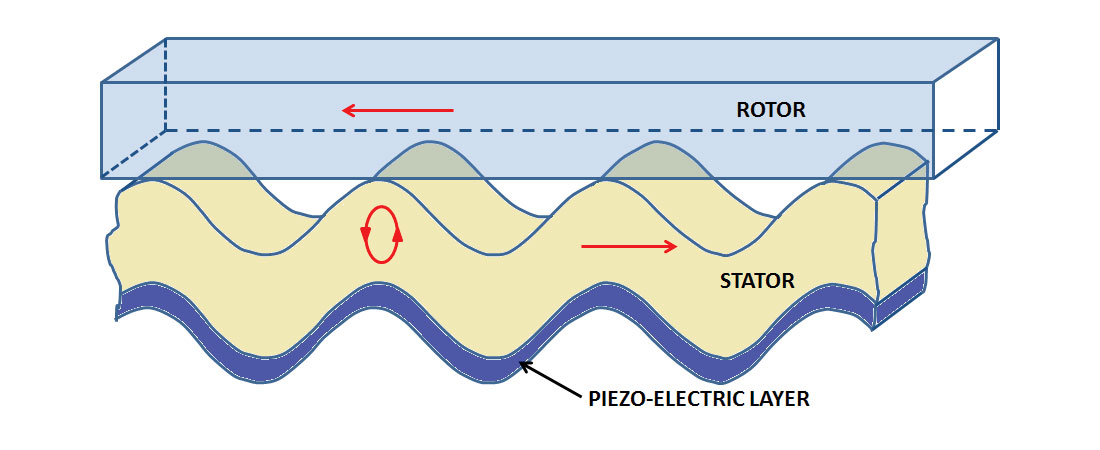
Image Sensor
Converting an image into pixels, encoded numbers representing specific colours, is the function of the image sensor. There is a very active debate about the relative merits of the different image sensor technologies in use. For many years charge-coupled device (CCD) sensors dominated, but lately complementary metal–oxide–semiconductor (CMOS) sensors are more commonly used. A number of factors have driven this shift. Both technologies were developed around the same time (~1970’s) but CCD’s were historically cheaper to produce and gave better images. However, as manufacturing methods advanced CMOS sensors became cost competitive, and they were more suited to the burgeoning phone camera market, due to lower power consumption. Also, over the years advancements have improved CMOS image quality greatly, and CCD’s no longer hold a clear advantage in this respect.
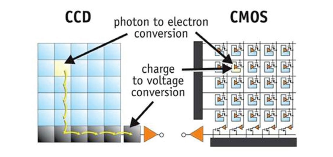
A CCD is a silicon chip with integrated circuits etched onto it, making up a 2D array of light sensors. Simplified, there are four layers: from top to bottom, a gate, glass insulators, an epitaxial layer made of p doped silicon, and finally a silicon substrate. When light (i.e. photons) hits one of these sensors, a number of electrons (proportional to the amount of photons received) are generated via the photoelectric effect. Because the gate on the other side of the insulators has been given a small positive charge relative to the other layers, the electrons are attracted to the gate and congregate next to the insulators which they can’t pass through. The CCD circuitry then passes each of these little “buckets” of electrons to its neighbouring pixel like a fire brigade; at the end of each row of pixels the “buckets” are passed in a similar fashion down columns, and this analog stream of voltages is sent to other circuitry to be amplified and digitized. The beauty of this scheme is that each pixel measures the light at exactly the same time, the entire area of each pixel’s silicon is devoted to sensing the light, plus the integrated circuitry is fairly simple and therefore easy to manufacture. The downside is that the predominantly serial method of analog harvesting is inefficient, with low bandwidth data bottlenecks.
The CMOS scheme is far more complex and I won’t attempt to describe it in detail. The light sensing aspects are essentially the same. The difference is that each pixel’s circuitry amplifies and digitizes the signal; because the outputs are digital the data can be moved off the chip much more quickly and efficiently. Figure 4 highlights this essential difference between CCD and CMOS. Interestingly, this advance is similar to what we experienced in seismic acquisition when distributed recording systems that digitized the seismic signals much closer to the geophones displaced central recording systems.
The advantages of CMOS sensors are that they are quicker (which facilitates many features now common on DSLR’s, such as panorama mode, exposure bracketing, HD video, etc.), use less power, and are now actually relatively cheap to make. Unlike CCD’s, CMOS image sensors do not actually simultaneously sense the light in all pixels at once like the CCD’s “global shutter”, instead they employ a “rolling shutter” system where the image is captured one row at a time, with about 1/100 of a second between scans. If the camera and/or the subject is moving, this can create distortion seen as a bending of the image’s moving elements. Before wrapping up I should address one aspect not touched on – colour. The way image sensors detect colour is actually fairly simple conceptually. Filters or masks at the surface of the chip separate the light signal into different bandwidths, say red, green and blue. Underneath there are arrays of pixels dedicated to each colour, so the sensor basically measures the amount of light in each bandwidth.
Photography is an extremely popular hobby, and the volume of information available on photography-related topics is staggering. I have just scratched the surface here. It is also a field with a large overlap between art and science, and tends to attract people who are passionate about the beauty of nature and the world around us. Thus it is no surprise that many geophysicists are enthusiastic and talented photographers. Just within my own small circle of CSEG friends I am aware of five very talented photographers: Wendy Mumma (https://500px.com/wmumma), Doug Pruden (www.prairielightimages.com), Marzena Feuchtwanger (https://instagram.com/marzif1/), Mark Ng, and of course RECORDER Editor Penny Colton; I’m sure there are others.


Share This Column